Soldering Defects in Electronics Manufacturing: Challenges Posed by Solder Bridges and alike
Scalable quality control with AI
Soldering defects are among the most common and costly quality issues in PCB manufacturing. But why are they so hard to detect? And how can modern AI help finally get this problem under control?
What are soldering defects—and why are they so critical?
Every electronic circuit board consists of a large number of components that are connected to one another electrically and mechanically via solder joints. These connections must be precise, complete, and free of short circuits—otherwise, the board will not function or, in the worst case, will fail after a short time.
Soldering defects can result from a variety of causes: temperature fluctuations in the reflow oven, incorrect settings during wave soldering, contaminants on the solder pads, misaligned components, etc.
The consequences range from occasional malfunctions to complete failure—which is particularly problematic when such errors go undetected and end up affecting the customer.
The Most Common Soldering Errors
The electronics manufacturing industry encounters a wide variety of soldering defects—the international standard IPC-A-610 provides a generally accepted framework for classifying and evaluating them. Among the most common defect patterns encountered in practice are:
Solder bridges
A solder bridge occurs when excess solder connects two adjacent traces or pins that are supposed to be electrically isolated from one another. The result is an unintended short circuit that can render the entire circuit board inoperable.
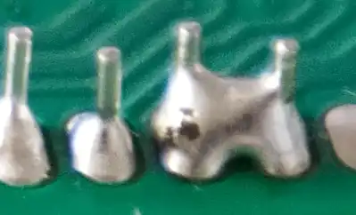
What makes them particularly tricky is that solder bridges never look the same. Sometimes they appear as a wafer-thin strand of solder between two SMD pins, and other times as a clearly visible solder bump between two pins. Their shape, size, and location vary from board to board, which causes problems for both manual and automated detection.
Missing pins
In through-hole assembly (THT), components are, as the name suggests, inserted through holes in the circuit board and soldered to the underside. If a component does not fit correctly into the designated holes—or hasn't beend placed at all—the corresponding pin will be missing on the other side.
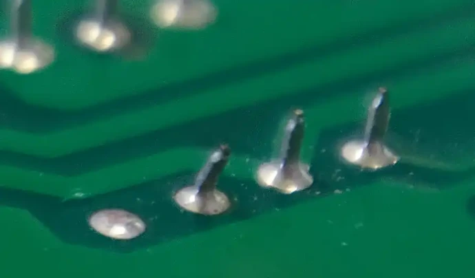
This isn't necessarily a direct soldering defect, but by properly inspecting the solder joints, you can detect the absence of THT components.
Cold solder joints
A cold solder joint occurs when the solder does not melt completely during the soldering process and no metallurgical bond is formed. The joint looks correct from a distance, but it is mechanically unstable and has high electrical resistance.

It may work at first and only fail weeks or months later—a classic warranty issue, especially if the circuit board has already been delivered and installed by then.
Tombstoning
Tombstoning is a soldering defect that occurs primarily with small SMD components. In this process, one end of the component detaches from the solder pad, causing the component to stand upright—like a tombstone. The cause is usually a thermal imbalance: if the solder paste melts faster on one pad than on the other, the resulting surface tension pulls the component to one side before both connections can solidify simultaneously.
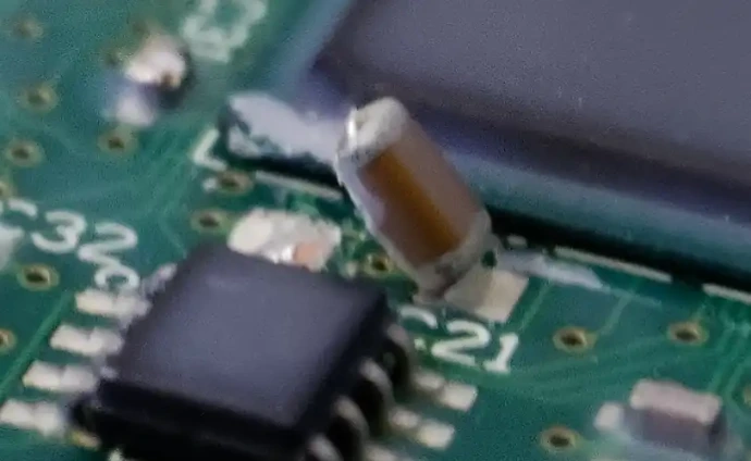
The result is a missing or broken solder joint—the circuit is open, and the component is non-functional. Especially on densely populated circuit boards, a misaligned component can easily be overlooked, particularly if it is located between larger components.
Solder deficiency and solder residue
Getting the right amount of solder is essential in industrial soldering: too little solder at a joint results in a weak or broken connection. Too much solder, on the other hand, can cause solder bridges or damage adjacent components.
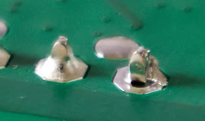
Flux residues that have not been properly removed can also become conductive when exposed to moisture, leading to leakage currents.
Limitations of manual visual inspection
The obvious solution: a person looks at the circuit board through a magnifying glass. This is an outdated approach that is impractical for several reasons:
Time and Cost: For circuit boards with hundreds or thousands of solder joints, a thorough visual inspection takes many minutes per unit. With high production volumes, this quickly adds up to enormous labor costs and creates a bottleneck on the production line that dramatically reduces throughput.
Subjectivity and Inconsistency: What Inspector A considers an “acceptable solder joint” may be rejected by Inspector B. Especially in borderline cases, such as weak solder bridges or slight solder shortages, there is no reliably consistent assessment. This leads to inconsistent quality and, in the worst case, to errors being systematically overlooked.
Non-specific defect patterns: Soldering defects often do not follow a standard pattern. A solder bridge may look different on one component than on another. It is difficult for the human eye to reliably detect this variability.
Scalability: As production volumes increase, manual testing simply cannot scale linearly. More circuit boards mean more testers—a model that is not economically viable in modern manufacturing environments.
AOI Systems: Automated Optical Inspection as the Solution
One approach to overcoming the challenges of manual visual inspection is to use an AOI system. Such systems typically run camera-based inspection programs that capture images of the solder joints and compare them with reference images.
The advantage is obvious: An AOI system never gets tired, always works with the same level of precision, and can inspect the solder joints on a circuit board in no time.
But even traditional AOI systems have problems with soldering errors: they operate using hard-coded thresholds and geometric rules and are therefore highly sensitive to normal fluctuations in the manufacturing process. This leads to high pseudo error rates: as a result, circuit boards are rejected as defective even though they are actually fine.
AOI with AI: A Breakthrough in Solder Joint Inspection
A modern approach involves combining high-resolution camera technology with AI applications in AOI systems. Instead of relying on fixed rules, an AI model learns from real-world images what correct and defective solder joints actually look like. It reliably detects patterns and anomalies even when they vary in shape and size. A solder bridge remains a solder bridge—regardless of whether it consists of a wide lump of solder or a thin thread. High-resolution cameras ensure that even the finest structures are clearly visible and analyzable—soldering defects that would simply escape the human eye.
One real-world example is ModSPOT. In a closed, controlled testing environment, a high-resolution camera mounted on an axis system systematically scans the inserted circuit board and analyzes each solder joint using an AI-based inspection program. This minimizes false positives—the system learns to distinguish between normal manufacturing variations and actual defects. The result: less scrap, less unnecessary rework, and consistently high quality.
AI for every use case
Building AI models often involves high costs. Service providers must be hired to train AI models using data that has been painstakingly collected. As soon as a new assembly is added or an existing one is modified, a new model must be trained, and you’re asked to pay up again.
You have more flexibility when you can create your own AI models. The AI-building tool ModOFFICE lets you create AI models yourself in just a few hours, without any programming knowledge. These models are ready to use right away and can be immediately integrated into inspection systems like ModSPOT, for example to detect soldering defects.
However, this also opens up the possibility of using the inspection systems for other applications, whether for testing protective coatings (which is no problem with UV lighting) or for inspecting THT and SMT components.
Conclusion
Soldering defects are a common and costly problem in electronics manufacturing. The sheer volume of defects makes manual visual inspection impractical from the outset, and traditional AOI systems reach their limits due to the irregular nature of the defects.
The combination of modern camera technology and AI-based image analysis bridges this gap: it detects soldering defects reliably, consistently, and quickly, without generating pseudo error. For PCB manufacturers looking to modernize their quality assurance processes, AI-powered AOI systems are no longer just a nice-to-have—they are a decisive competitive advantage.
Author: Frederick Warken